Product description

Product model

Design & development

  • CMS8S69xx

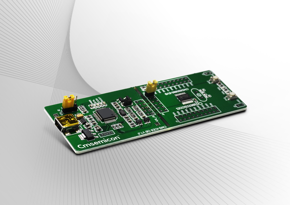
    Enhanced 1T 8051, 16KB Flash, the fastest 48MHz peripheral operation, dual op amps, dual comparators, PGA, free mapping of digital functions. The CMS8S69xx series of MCUs have a wealth of analog peripherals, which can simplify the peripheral circuit of the product, and are widely used in various application fields such as e-cigarettes, wireless charging, mobile power supplies, motor controls, wireless light control, TWS headset charging bins, personal medical care, security, etc. 


    Datasheet >

    CMS8S69xx is an enhanced 1T 8051 Flash MCU, the fastest support 48MHz peripheral operation, 24MHz core operation, working voltage 2.1V-5.5V, GPIO up to 22, built-in 2 analog comparators, 2 operational amplifiers, 1 channel Programmable gain amplifier, providing 6-channel complementary PWM output with dead zone control, up to 22 channels of 12-bit ADC, 2 UARTs, 1 SPI, 1 I2C. Industrial standard design, can work at -40℃ to -105℃, and provide SSOP20, TSSOP20, QFN20, SSOP24 and QFN24 packages.


    Features

    > Enhanced 1T 8051

    > Working voltage: 2.1V-5.5V @Fsys=48MHz, Fcpu=24MHz

    > Working temperature: -40℃-105℃

    > Working frequency: Fsys=48MHz, Fcpu=24MHz

    > Built-in 16KB Flash ROM (support BOOT function area, 0K/1K/2K/4K optional), 1KB Data Flash, 256B general RAM, 1KB general XRAM

    > Support 4 different oscillation modes

    > Up to 22 general GPIOs, all digital functions can be assigned to any GPIO

    > 2 analog comparators, offset voltage less than ±1mV

    > 2 operational amplifiers, offset voltage less than ±1mV

    > 1 programmable gain amplifier, offset voltage less than ±200uV

    > up to 22 channels 12-bit ADC, built-in 1.2V reference voltage, reference Voltage optional 1.2V/2.0V/2.4V/3.0V/VDD

    > 5 16-bit timers, Timer2 has Capture/Compare function

    > Built-in WDT timer

    > Built-in LSE timer, support sleep wake-up function

    > 2 UART serial ports , the baud rate is up to 1Mb/s

    > 1 SPI, the communication rate is up to 6Mb/s> 1 I2C, the communication rate is up to 400Kb/s

    > 6 channels of 16-bit enhanced PWM, supporting independent and complementary modes and programmable dead zone delay, PWM output port can be multi-port mapping

    > Built-in low voltage reset function (LVR): 1.8V/2.0V/2.5V/3.5V

    > Built-in low voltage detection function (LVD): 2.0V/2.2V /2.4V/2.7V/3.0V/3.7V/4.0V/4.3V

    > Beeper> 96bit unique ID (UID)

    > Package: TSSOP20, QFN20, SSOP24 and QFN24


  • Product model

    Part Number Package Frequency (MHz) Core Temp Voltage Memory Type ROM RAM Data Flash EEPROM GPIO DMA Timer LSE WDT/WWDT RTC UART I²C SPI CAN LIN PWM/EPWM SAR-ADC SAR-ADC-bit SAR-ADC-ch SAR-ADC-speed(Msps) DAC DAC-bit OPA COMP PGA LCD LED Touch Encryption Other Interface
    SAR-ADC-unitSAR-ADC-bitSAR-ADC-chSAR-ADC-speed(Msps)DAC-unitDAC-bit
    CMS8S6980 SSOP20 48 8051 -40~105 2.1~5.5 FLASH 8KB 256B+0.5KB 1KB / 18 / 5x16 Y / / 1 1 1 / / 6 1 12 18 / / / / 1 /

    /

    /

    / / /
    CMS8S6990 QFN24 48 8051 -40~105 2.1~5.5 FLASH 16KB 256B+1KB 1KB / 22 / 5x16 Y / / 2 1 1 / / 6 1 12 22 / / / 2 2 1

    /

    /

    / / /
    CMS8S6990 SSOP24 48 8051 -40~105 2.1~5.5 FLASH 16KB 256B+1KB 1KB / 22 / 5x16 Y / / 2 1 1 / / 6 1 12 22 / / / 2 2 1

    /

    /

    / / /
    CMS8S6990N TSSOP20 48 8051 -40~105 2.1~5.5 FLASH 16KB 256B+1KB 1KB / 18 / 5x16 Y / / 2 1 1 / / 6 1 12 18 / / / 2 2 1

    /

    /

    / / /
    CMS8S6990NA QFN20 48 8051 -40~105 2.1~5.5 FLASH 16KB 256B+1KB 1KB / 18 / 5x16 Y / / 2 1 1 / / 6 1 12 18 / / / 2 2 1

    /

    /

    / / /

  • Design & development

Tel
+65-64633764
Address
#05-10, Connexis North
Singapore 138632
Email
general@Changitech.com

This site uses cookies. By using our site you agree to our privacy policy. By closing this banner, scrolling this page, clicking a link or continuing to browse otherwise,you agree to the use of cookies.