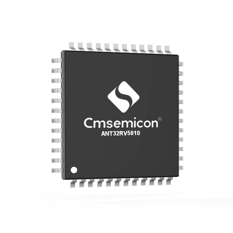
ANT32RV56xx has built-in 2 operational amplifiers and 2 comparators, 2 programmable gain amplifiers, which can replace off-chip operational amplifiers and comparators for wireless charging and decoding circuits. It can quickly provide effective protection against abnormal situations in system control. The chip has two built-in high-precision 12-bit ADCs, low-speed and high-speed, which can accurately collect voltage, current and temperature signals for system control for different application scenarios; The flexible configuration of enhanced PWM is suitable for half-bridge and full-bridge control, and the fast braking function can effectively protect the entire control system.
> RISC-V core 48MHz@2.1V~5.5V
-RV32EC instruction architecture
> Memory
-64KB Flash, 1KB Data Flash, 32KB ILM-SRAM, 8KB DLM-SRAM
-Support BOOT function, space can be set to 0~4KB
> Flexible configuration The system clock can be switched freely
-Internal high-speed RC oscillation: 48MHz
-Internal low-speed oscillation: 40KHz
> Abundant timers
-1 24-bit timer
-4 32-bit/16-bit optional general-purpose timers
-1 32-bit watchdog timer
-1 6-bit window watchdog timer
> 32-bit hardware divider
-with unsigned mode, 6 clock cycles completed
> built-in high-precision temperature sensor
> dedicated PWM module for motor control
-Support independent/complementary/synchronous/group output mode
- Support center symmetrical and asymmetrical mode
- Support single/continuous/interval loading mode
- PWM port line with remapping function
- Any edge or period of PWM can trigger ADC conversion
- Support Wave-by-wave current limiting PWM function
> High-precision 12-bit ADC-Built
-in 1 low-speed 12-bit ADC@100Ksps-Built
-in 1 high-speed 12-bit ADC@1.2Msps
-Both low-speed and high-speed ADCs use 12 external channels, 8 Internal channel architecture
-Each channel has an independent result register
> Abundant analog peripherals
-Built-in 2 high-performance operational amplifiers (10MHz, 10V/us)
-Built-in 2 high-performance analog comparators, support bilateral hysteresis function (10mV /20mV/60mV)
-Built-in 2 PGA, 4~32 times gain optional
> Support general cyclic redundancy check unit (CRC)


